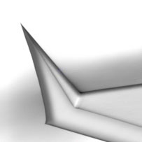
AFM Standard
AFM Standard
The cantilever is a key element of any scanning probe microscope, the properties and quality of which depends on the successful operation of the microscope in General. This is the basic measuring element of many types of probe microscopes. The right choice of the cantilever is one of the most important conditions for obtaining good AFM images.
The most important component of AFM (Atomic force microscope) are the scanning probes of the cantilevers. The cantilever is a flexible beam (175х40х4 µm — average data) with a certain stiffness coefficient k (10-3 – 10 N/m), which is a micro needle.
TipsNano company offers a wide range of cantilevers for a wide range of applications of scanning probe microscopy and full research samples.
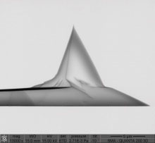
AFM Special
AFM Special
The cantilever is the most common sensor of the force interaction in atomic force microscopy. Any information about the surface atomic force microscope receives due to mechanical deflections of the cantilever beam, which are detected by an optical system. The AFM image in this case describes the spatial distribution of forces of interaction of the probe with the surface.
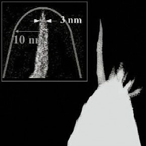
SNOM
SNOM — scanning near-field optical microscope, scanning near-field optical microscopy. In near-field optical microscopy uses different principles of construction of the image of object, which allow to overcome the difficulties associated with diffraction of light and to realize a spatial resolution of 10 nm and better. Higher resolution Bohm is achieved by detecting scattering of light from the object under study at distances smaller than the wavelength of light. In the case that the probe (detector) of the near-field microscope provided with a device for the spatial scan, the scanning device called optical near-field microscope. This microscope allows to obtain a raster image of surfaces and objects with a resolution below the diffraction limit.
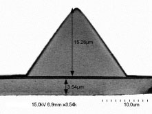
HOPG
HOPG
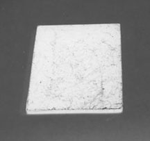
TipsNano supply with Highly Oriented Pyrolytic Graphite (HOPG). It’s a type of pure, highly laminar graphite used as an atomic-scale calibration standard for atomic force microscopy and scanning tunnelling microscopy.
HOPG crystals are widely used as substrates in STM (Scanning Tunneling Microscopy). The most distinguishing features of HOPG which enable this application are a very smooth surface and electro conductivity.
HOPG has a layered structure which makes sample preparation very simple. By pressing a double-stick tape to a HOPG piece and peeling it off, one gets a fresh conductive surface which is very smooth. This surface can be examined in STM or serve as a substrate for other materials under investigation.
HOPG itself is an interesting object for STM investigations. One can measure the surface roughness, microscopic surface features, arrangement of the carbon atoms on the HOPG surface, etc. Besides, HOPG images at the atomic level can be used for calibrating STM for high-resolution imaging.
4 HOPG types (ZYA, ZYB, ZYD, ZYH) which differ by meaning of mosaic spread are available with sizes till 50x50mm. Both double-sided (DS) and single-sided (SS) HOPG pieces can be ordered.
Double-sided HOPG can be used from both sides and its properties are not changed in depth.
For one-sided piece the not working side is mat, glare less and can’t be cleaved. The number of working side cleavages of one-sided piece is limited in comparison with double sided substrate. The properties for one-sided piece are changed in depth.
Calibration
Calibration
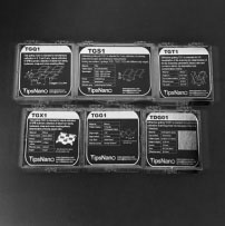
To determine the credibility of studies by AFM — microscopy testing and calibration of microscope work and test the quality of probes (scale of X-, Y-, Z – coordinates, the radius of the tip of the cantilever, linearity and orthogonality of the axes of the scan). For calibration and determination of the working shapes of the probes used special test structures with known topography.
For the calibration of microscopes in the scanning plane and vertically apply a diffraction grating with submicron sizes. In the absence of a specially manufactured calibration gratings, can be used as a test object to obtain atomic resolution fresh cleaved mica or highly oriented pyrolytic graphite (HOPG), because the parameters of the terrain are well known.
Advantages of graphite as the test sample are: stable operation is output; a low concentration of point and line defects; low reactivity in atmospheric conditions; the possibility of obtaining atomically clean surface.
TERS
TERS
TERS — Raman Spectroscopy with the enhancement of the tip. Measurements based on AFM microscopy. Mode TERS Raman spectrum is enhanced when a sharp tip with a gold coating approaches the illuminated sample surface. Using the cantilever of an AFM as an amplifier, measure the chemical properties of the sample in the nano-range by using the built-in Raman spectrometer, simultaneously obtaining topographic data by using ASM.
